Seminar “Characterisation of single semiconductor nanowires by non-destructive spectroscopies”
Date
Tuesday, 6 September 2016
Time
12:00 am
Place
University of Barcelona
Faculty of Physics Building
Room 3.20, 3rd floor
Speaker
Dr Eleonora Secco, Institute of Material Science, University of València (Spain)
Abstract
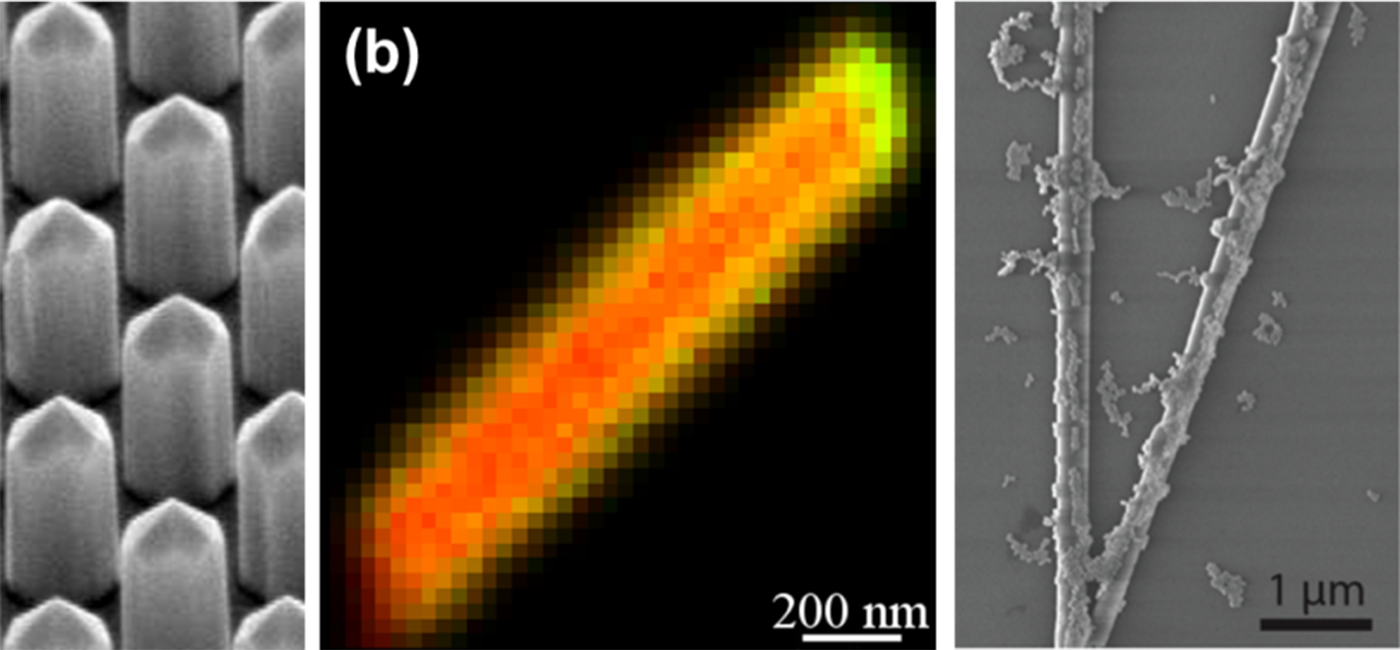
Semiconductor nanowires (NWs) have a broad range of potential applications in the field of optoelectronics (light-emitting and laser diodes), nano-electronics (logic circuits and field effect transistors), sensing, and energy harvesting (solar cells) [1]. Many semiconductors have been obtained in the form of NWs by means of different growth techniques and aiming at different applications [2]. In particular, the materials that will be presented in this seminar, ZnO, GaN, and GaN-based alloys (InGaN) are favorable for short-wavelength light emitting devices, high-power devices and photovoltaic solar cells [3, 4, 5].
The advent of nanotechnology has brought with it not only an outstanding number of potential applications in many fields but also the need for characterisation techniques capable of correlating the fundamental properties of the nanostructured materials and the performance of the devices.
The study of single and ensemble of NWs introduces new challenges to carefully and efficiently characterise devices and samples. The properties of the device will be those of an ensemble of many individual NWs. While, single NWs can present slight differences in their optical properties and therefore they exhibit their own individual spectra. Performing single NWs studies is the only way to univocally evidence their individual properties. Thus, techniques that enable the study of ensembles as well as single NWs with spatial resolutions ranging from the micro- to the nano-scale are required. Moreover, in nanoscale functional materials, it becomes very important to determine the relationship between structural and optical properties. This requires the application of different techniques to the same nano-object.
Therefore, it is mandatory the use of non-destructive and contact-less spectroscopic techniques, which do not require a special preparation of the sample and allow performing several experiments on the same NWs.
In this talk, I will provide an overview of my entire career trajectory, spanning from my Master’s Degree in Physics to my postdoctoral experience. I will pay special attention to the research on semiconductor NWs I carried on (by means of optical and X-ray spectroscopy, and atomic force microscopy) during my PhD at the Institute of Materials Science of the University of Valencia.
References:
[1] Wei Lu and Charles M Lieber. Semiconductor nanowires. Journal of Physics D: Applied Physics, 39(21):R387, 2006.
[2] Matt Law, Joshua Goldberger, and Peidong Yang. Semiconductor nanowires and nanotubes. Annual Review of Materials Science, 34(1):83, 2004.
[3] Yangyang Zhang, Manoj K. Ram, Elias K. Stefanakos, and D. Yogi Goswami. Synthesis, characterization, and applications of ZnO nanowires. Journal of Nanomaterials, 2012:624520, 2012.
[4] Shunfeng Li and Andreas Waag. GaN based nanorods for solid state lighting. Journal of Applied Physics, 111(7):071101, 2012.
[5] Bryan M. Wong, François Léonard, Qiming Li, and George T. Wang. Nanoscale effects on heterojunction electron gases in GaN/AlGaN core/shell nanowires. Nano Letters, 8(11):3074, 2011.